3-D e-Beam Lithography
Motivation:
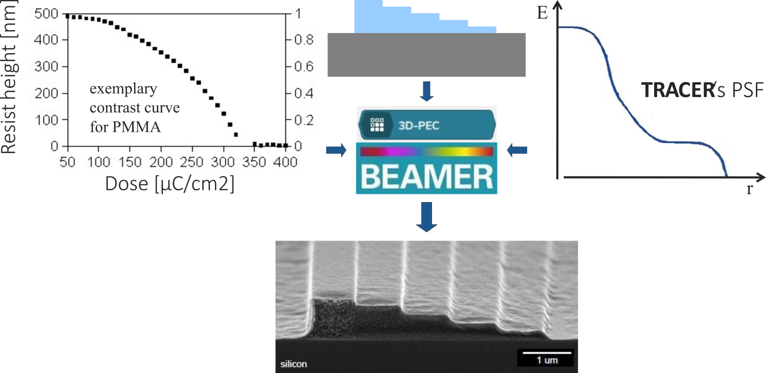
A growing demand for fabrication of 3D nanostructures like diffractive optical elements or computer-generated holograms require a complex data-preparation to define the post-development resist thickness at all positions. Since resist thickness depends on the development process (as described by the contrast curve and the absorbed energy at a given position) and the layout density condition, experimental trial & error optimisation is not feasible as the number of parameters and interactions is very large.
Solution:
BEAMER 3D PEC module makes 3D e-beam lithography very easy. The user can import the experimentally determined contrast curve of the resist development process, the PSF (e.g. from Monte Carlo - TRACER simulation) and the layout with the target resist thickness encoded as layers. BEAMER calculates the target absorbed energy and applies PEC for computing the required doses. The result is a dose corrected layout, which is exported to a desired tool format and exposed.