Electron- and Laser-Beam Lithography Software
Optimum productivity, quality and innovation by advanced data preparation for electron- and laser-beam lithography systems
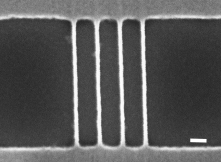
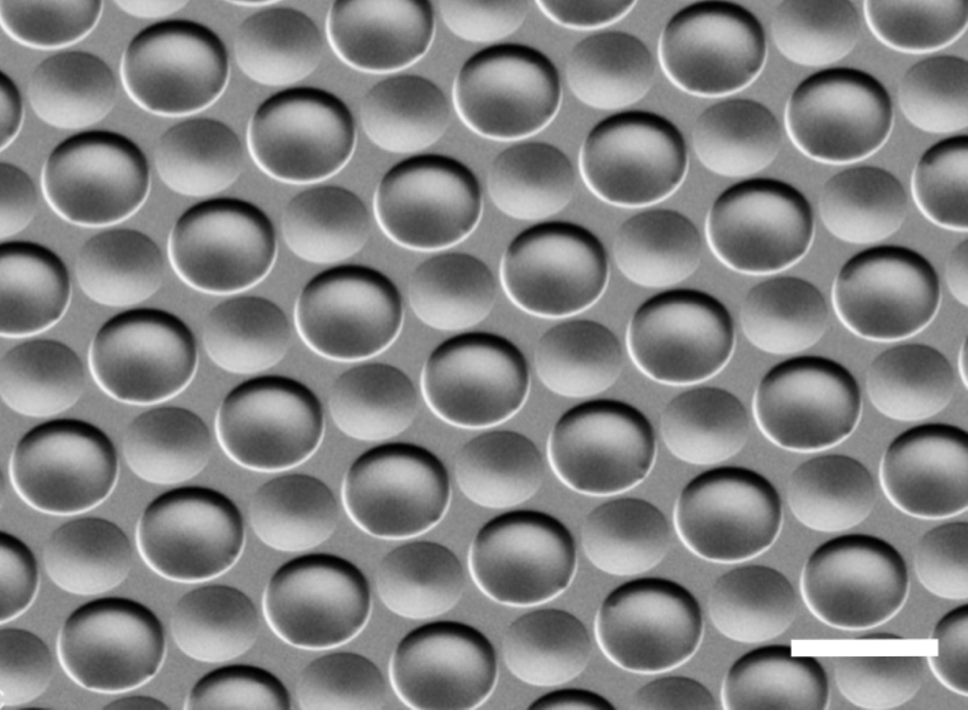
High-resolution and high-throughput electron-beam lithography is severely impacted by process effects, electron scattering effects, and tool artifacts resulting in non-ideal pattern transfer. Although the electron-beam tool is a highly sophisticated and expensive printer, the pattern data needs to be optimized to significantly reduce the effects of various error sources such as beam positioning between shapes, filling shapes with “shots” on a discrete grid, field position dependent aberrations, stitching between fields, the spread of energy by electron scattering (proximity) and process effects.
BEAMER is the most comprehensive lithography software for optimum electron and laser-beam exposure:
- Support for all major electron- and laser-beam exposure systems
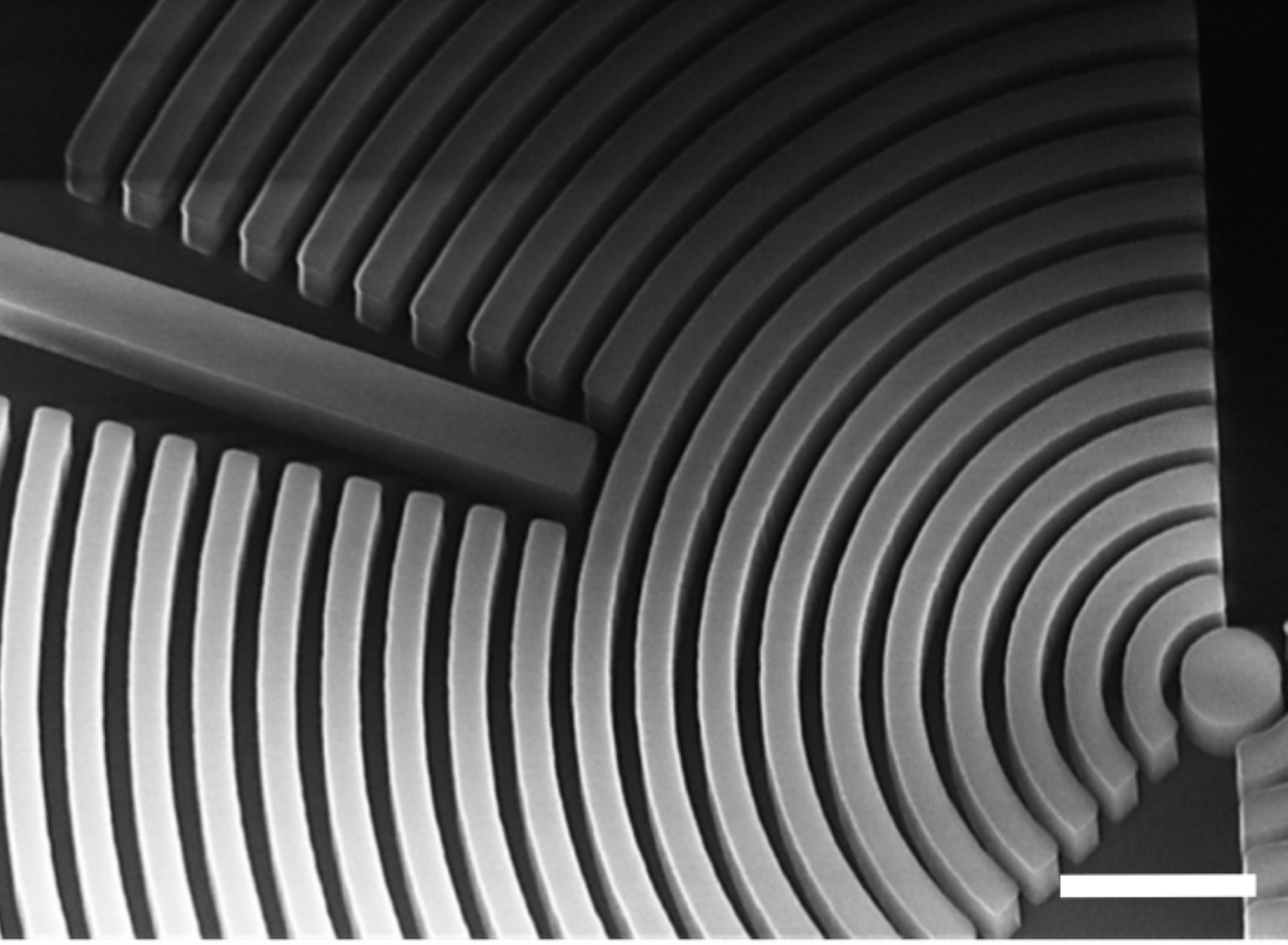
- Superior machine specific fracturing of complex curved layouts
- Optimized field and shot placement
- Writing order control and advanced writing strategies
- Library of comprehensive layout processing functions
- Support for all major layout formats
- Integrated layout editor
- Built-in Viewer for immediate inspection, verification, and measurement of patterns
- Powerful proximity and process effect correction technology
- Electron-beam simulation of absorbed energy and resist contours
Productivity, Quality & Innovation
BEAMER provides reliable and highly powerful processing of large and complex layout data. It gives the user a large array of functions for extracting, combining and modifying the layout for an optimum exposure. Interfaces for all major electron and laser-beam exposure tools are developed in close cooperation with machine vendors and are continuously optimized for the best exposure results, thereby extending the limits of these systems by advanced data preparation. Examples include: optimized fracturing for a significant reduction in shot placement artifacts, automated floating field to avoid /reduce field placement and stitching issues, user controlled field placement, and enhanced multi pass
strategies. The user can instantly visualize and quickly optimize the exposure process, including field and shot position. Applying techniques such as “bulk & sleeve” or “coarse & fine” combined with proximity effect correction (PEC) to easily and effectively achieve high resolution, smooth edges at increased throughput.
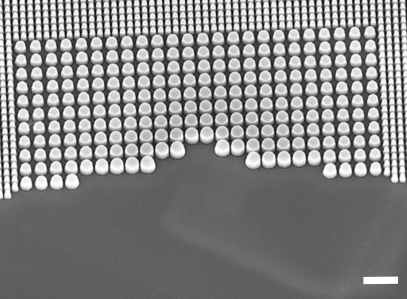
PEC is essential for improving the exposure quality by automatically adjusting exposure doses for optimum CD (critical dimension) uniformity and contrast. Additionally, PEC eliminates the need to experimentally adjust the exposure dose for each layout thereby increasing productivity and process reproducibility. Performing traditional “Trial & Error” optimizations is very expensive and time consuming.
Advanced techniques available include: “model-based undersize-overdose” enabling ultra-high resolution in difficult scenarios, 3D PEC for three dimensional resist profiles in single and multi-layer resists, and full process calibration with simulation for quick development of new innovative solutions.
Strong collaboration with leading nanofabrication centers worldwide drives rapid enhancements and allows us to provide the most advanced capabilities to our users, improving their efficiency and effectiveness. BEAMER is designed for the industrial user focused on productivity, as well as universities and R & D centers interested in flexibility and high resolution lithography.
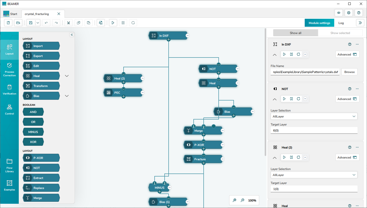
The VisualFLOW™ user interface allows fast process flow creation by simple drag & drop to connect functional modules, providing increased productivity and efficiency.
A comprehensive library of modules is available for building powerful flows. User Libraries allow storage and easy re-use of common blocks of modules for often-used functions.
The integrated VIEWER provides layout inspection at all stages, comparing layouts in multi-view mode, measurement functions, metrology support, writing field placement, dose assignment, and shot placement. VIEWER is also available as a stand-alone software package.
BEAMER includes Import /Export for all major layout and machine formats, without size limitations. The integrated Layout Editor allows the creation and /or modification of layouts. The machine formats are continuously enhanced in strong cooperation with the machine vendors, to provide the best possible exposure results. Examples of advanced machine features include: optimal fracturing of complex curved layouts, flexible control of field placement and shot placement, writing order definition and control, compensation for tool artifacts by intelligent multi-pass, and powerful data compaction.
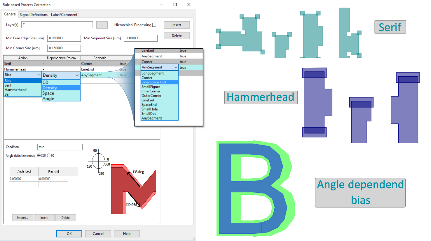
BEAMER provides innovative tools for PEC and advanced process correction for nanoscale electron-beam lithography. A robust 2D PEC is complemented by a model-based shape and rule-based corner correction, plus correction for 3D correction for 3D single and multi-layer resist profiles. The flexible Point Spread Function (PSF) calculated by TRACER, can
extend to correcting substrate, resist, and other process effects. Rule-OPC allows angle, size, or density dependent biasing and placement of resolution enhancement features for laser-beam lithography, and mask making in general. Rule-OPC allows angle, size, or density dependent biasing and placement of resolution enhancement features for laser lithography, and mask making in general.
BEAMER integrates electron-beam simulation, allowing for verification and optimization via modeling of the corrected layout. The modeling includes beam positioning for the major electron-beam systems. The combination of Metrology for comparing simulated with experimental data, along with the Optimizer, facilitates the adjustment of model PSF parameters to perform basic process effect correction. The TRACER software package, in combination with BEAMER, allows full process calibration and correction, including not only exposure effects, but also development, process and metrology effects.
BEAMER Major Features
Layout Import / Export:
- Layouts of all major formats, without size limitation (GDSII, CIF, DXF, LTXT, OASIS, BMP, DWG)
- Electron- and laser-beam machine formats (Raith, JEOL, Elionix, Crestec, ADVANTEST, MEBES, Vistec, Heidelberg)
Advanced Fracturing:
- Support of all major machine formats
- Optimized for arbitrary shapes
- Curved fracturing
- Correction for shot positioning
- Beam Step Size (BSS) fracturing
- Field position control (tiled, floating, manual)
- Multi-pass exposure
- Writing order control
Integrated Layout Editor:
- Create new layouts
- Edit layout within flow
VIEWER:
- Integrated detachable global viewer
- Multi-view
- Feature Measurements
- Shot and field placement view
- Write order and field visualization
- Dose assignment
Layout and Boolean Operation:
- Healing, Biasing, Sizing, Merge, Tone reversal (NOT)
- AND, OR, XOR, P-XOR, MINUS
- Extract layer, datatype, cell, region
- Scale, Shift, Rotation, Mirror
- Filter geometries by width, height, area, angle, and relative dose
- Grid adjustment
- Mapping layout layers and datatypes
- Pre-fracture
- Cell Replace
- Hierarchy Flatten or Build
Flow Control Modules
- Parametrized loops with IF, SELECT, and FILTER operations
- Script for starting command line application from flow
- Optimizer for parameter fitting
Proximity and Process Correction
2D Dose PEC
- Fast and robust edge equalization technique
- Excellent dimension control by optimized dose on feature edges
- Fracturing based on absorbed energy distribution
- Perfectly symmetrical and stable for arbitrary shapes
- Process correction (e. g. lateral development, loading)
Shape Correction
- Model based shape correction of short and mid-range effects
- Combination with long-range correction with dose modulation
- Model based contrast enhancement (“undersize – overdose”)
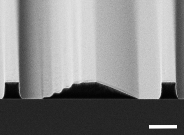
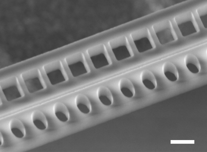
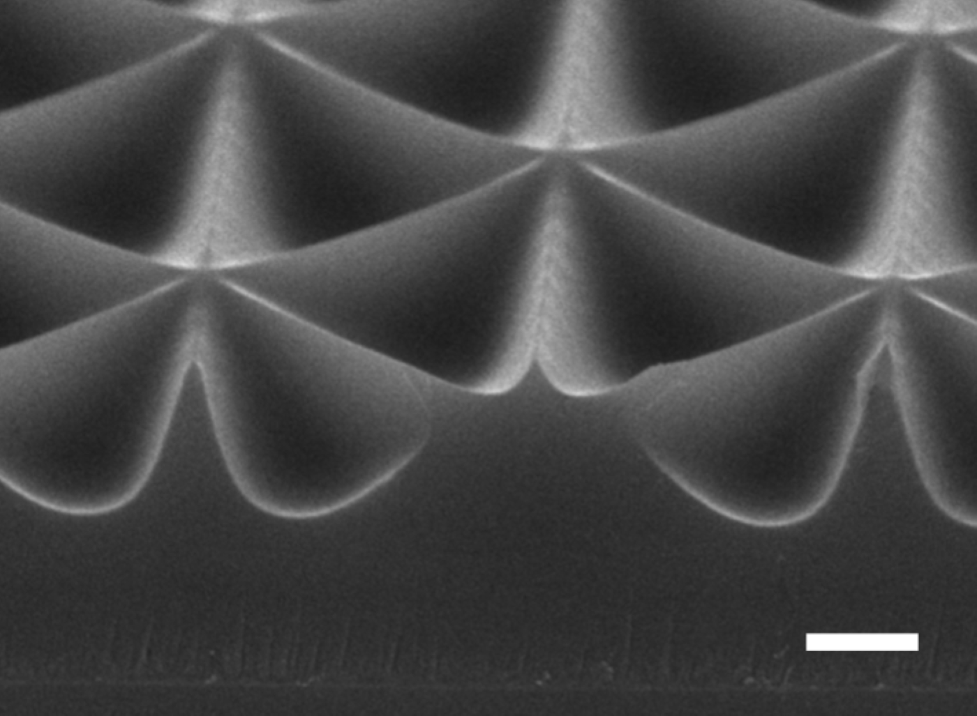
3D PEC
- Correction for defined resist thickness at any layout position (resist profile) for single layer resist (e.g. 3D gratings, 3D holograms, angled sidewalls, lenses)
- Correction for critical dimensions (CD) for each layer for a multi-layer resist (e.g. T-gate structures)
- Additional compensation for substrate topography or material variation
Laser-beam Lithography Correction
- 3D Gray Tone Lithography
- OPC for resolution and linearity enhancement
Corner PEC
- Corner sharpening correction
- Dose PEC combined with rule-based correction for edges, inner and outer corners.
Flexible PSF and Process Modeling
- PSF from Monte Carlo simulation or experimental table
- Visualization and fit of PSF function
- Apply full PSF data or Gaussian approximation
- Process loading, shot size dependent blur, fogging effect
Electron-beam Modeling
- 2D intensity image, 2D resist contour at multiple thresholds
- 1D / 2D image viewing and analysis
- Multi- and matrix-view for automated runs
- Metrology for automated measurement and comparison to experiment
- 3D resist simulation can be performed with the LAB software package
GenISys products share highly dedicated support, have flexible licensing and are available on various platforms/operating systems.
Flexible licensing and platform support
- USB license key for standalone and network
- Flexible on off-the-shelf PCs (> 4 GB RAM recommended)
- Windows 10 64bit, Linux64bit (Red Hat 6+, Ubuntu 18.04)
- Multithreaded processing
Maintenance and Support
- Technical Support Hotline (e-mail, screen sharing or phone)
- Frequent updates with new features, enhancements and bug fixes
- Regional trainings, technical workshops and user meetings
- 12 months maintenance service included in license price
- User feature requests are given high-priority for future updates
New Features in Latest Versions